
Online Gerber Viewer: Why You Need a Proper Gerber Viewer
Free · 100% Local · No Install · 30 Languages
First, What is Gerber?
If you're not in the PCB industry, hearing "Gerber file" for the first time might sound cryptic.
Put simply, a Gerber file is the "blueprint" your PCB fab uses to build your board. When you finish your schematic and layout in KiCad, Altium, or Eagle, the files you export for manufacturing are Gerber files. Each file describes one layer — where the top copper traces go, how big the solder mask openings are, where the silkscreen labels sit, where the drill hits land. The fab's CAM engineer reads these files to set up the production line.
The industry standard is RS-274X, also called Extended Gerber, an open format maintained by Ucamco. There's also Excellon, a format dedicated to drill data, originally defined by TTL back in the 1970s — and it's still the universal language for CNC drilling machines today.
A typical PCB project ships with 7 to 20 individual files. A 4-layer board alone needs at least 4 copper layers (top, inner 1, inner 2, bottom), plus top solder mask, bottom solder mask, top silkscreen, bottom silkscreen, outline, and drill — it adds up fast.
The question is: how do you know all these files are correct before sending them off?
The Awkward Reality of PCB Review
Before the fab actually builds your board, you need to verify three things:
- No export errors — you might have added teardrops in KiCad but forgotten to enable them in the Gerber export options
- Layers are aligned correctly — the offset between drill holes and pads must stay within manufacturing tolerances
- The fab can read your files — different CAD tools produce Gerber with subtle format differences, and not every fab's CAM system handles every dialect equally
This forces every PCB designer to "preview" their Gerber through some viewer before hitting the "order" button.
But honestly, the options on the market each have their own frustrations:
Desktop tools:
- GC-Prevue (formerly GraphiCode) — solid tools, Windows-only, UI stuck in the 90s, commercial license isn't cheap
- ZofzPCB — nice 3D rendering, but only supports bare copper layers — no solder mask or silkscreen overlay
- gerbv — open-source, cross-platform, but the UI is bare-bones, the interaction feels clunky, and measurement features are almost nonexistent
- CAM350 — industrial-grade, but that's what fabs use. Individual designers shouldn't have to install a monster like this just for a quick look
- KiCad/Altium/EAGLE built-in preview — convenient, but previewing Gerber in the same tool that exported it means you're "checking your own work." It's easy to miss export-specific issues. Plus, not everyone has a multi-gigabyte EDA suite installed
Online tools:
- Tracespace Viewer — open-source online viewer with a solid parsing engine (we borrowed from it too), but feature-light: no measurement, no grid overlay, no multi-language UI. Inspecting complex boards lacks practical aids
- EasyEDA Viewer — tied to the EasyEDA ecosystem, half-online flow, not a general-purpose viewer
- Altium 365 Viewer — web-based Gerber viewing, but requires an Altium account, files must be uploaded to their cloud, and the whole experience is deeply tied to the Altium ecosystem. High barrier if you just want to peek at a file
Shared Project PCB editors (Altium 365, Upverter, etc.):
- All require uploads, registration, and accounts. Opening a file often takes multiple clicks — nowhere near as simple as drag-and-drop
The common problems across all of them:
- Upload required — trade secrets, unpublished designs, sensitive projects — sending files to someone else's server never feels quite right
- Install required — hundreds of megabytes or even gigabytes of installer. Switch computers and you have to do it all over again
- Registration required — email, account, password — a hassle
- Paid — hobbyists, students, small teams don't want to pay for something they only use occasionally
This is exactly why I built Online Gerber Viewer: a Gerber browser that just works, and asks nothing from you.
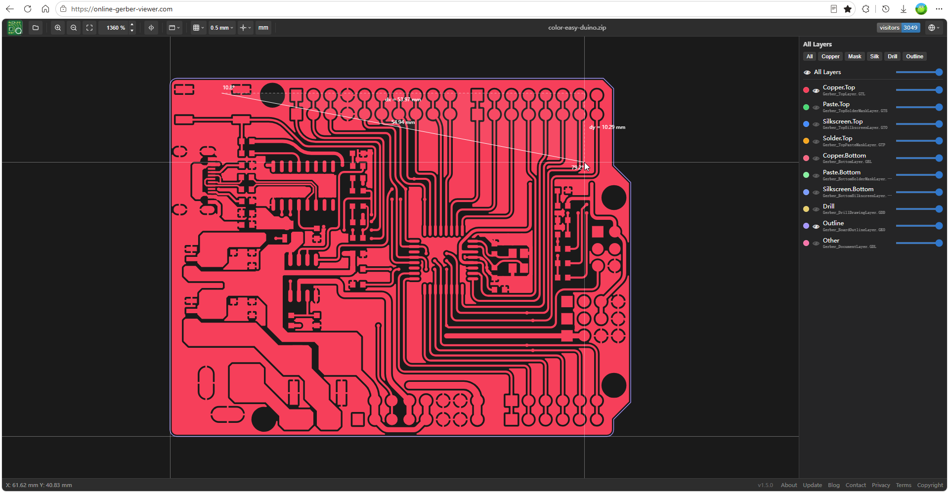
What It Solves
📂 File Loading: Just Drag It In
No registration. No "New Project" dialog. No template selection.
Drag your Gerber files straight into the browser window, or click the folder icon in the toolbar — that's it. Got a ZIP archive? Drag the ZIP in directly. It auto-extracts, filters out irrelevant files (macOS __MACOSX directories, JSON files, images, PDFs — all skipped automatically), and picks out only the Gerber and Excellon files.
A progress bar shows you the loading status, and non-PCB files trigger a friendly toast notification without interrupting the flow.
Just want a quick look? Click the "Example Files" button in the toolbar — the built-in color-easy-duino board loads instantly.
Single file cap is 100 MiB, which is generous for Gerber — even a complex 12-layer board typically clocks in at 10–30 MB for all layers combined.
🎨 Layer Identification: 19 CAD Tools, Auto-Classified
Different CAD tools produce wildly different Gerber filenames:
| CAD Tool | Top Copper | Top Silkscreen | Drill File |
|---|---|---|---|
| KiCad | project-F.Cu.gbr |
project-F.Silkscreen.gbr |
project.drl |
| Altium | project.GTL |
project.GTO |
project.TXT |
| Eagle | project.CMP |
project.PLC |
project.DRL |
| OrCAD | project.TOP |
project.SST |
project-1-4.drl |
| DipTrace | project.ph1 |
project.pt1 |
project.drd |
Online Gerber Viewer uses a majority-vote algorithm: it scans every filename you drop in, tallies which CAD tool's naming patterns match most frequently, then uses that tool's rules to identify each layer precisely. For example, if it sees .GTL, .GBL, .GTS, .GBS together, it automatically recognizes this as an Altium project and classifies accordingly.
Supported CAD tools: KiCad, Altium Designer, Cadence Allegro / OrCAD, Autodesk Eagle (Legacy / OSH Park / PCB-ng variants), DipTrace, gEDA PCB, Siemens PADS, Proteus, Pulsonix, DesignSpark, EasyEDA, CircuitMaker, CircuitStudio, Target 3001!, Zuken CR-8000 / BoardStation, Mentor Expedition, P-CAD.
After identification, layers are automatically grouped into: Copper (top / inner / bottom), Solder Mask, Silkscreen, Solder Paste, Drill, Outline. Each layer shows a color dot on the right panel for quick visual reference.
🔍 Visual Inspection: What You Actually Need
PCB review is fundamentally about "stacking layers and looking through them." The layer panel delivers this:
- Independent show/hide per layer — view only top copper and drill to check pad-to-hole alignment
- Per-layer opacity control — when stacking layers, crank up transparency to see traces underneath
- Global filter buttons — one click to show only "Copper" or only "Drill" layers instead of toggling each one
- Customizable layer colors — 28 presets for quick picks, plus an eyedropper tool to sample any color from the screen. Great for color-coding different functional nets
🔄 Zoom, Pan, Flip
- Zoom range 1%–20,000% — from full-board overview to zooming in on a single via
- Scroll-wheel zoom and drag-to-pan — as intuitive as a map app
- Fit-to-view — centers the entire board in one click
- Horizontal flip — inspecting traces from the reverse angle often reveals routing issues. This isn't a simple image rotation — it mirrors the entire canvas coordinate system, which works correctly with layer stacking
📏 Measurement
Gerber files carry no dimension annotations — a virtual caliper is essential.
Click the measurement tool, pick two points on the canvas, and it displays:
- Distance between points
- X offset (dx)
- Y offset (dy)
- Included angle
Units can be toggled in real-time between mil (thousandths of an inch — the PCB industry standard) and mm. All labels update automatically.
Continuous measurement mode is great for measuring a row of via pitches in one go, or segmenting a long trace run.
Measurements run on an independent Canvas overlay, so they never interfere with the PCB rendering underneath. Labels scale correctly with zoom.
🎯 Grid
PCB layout is fundamentally grid-aligned — pads on grid, traces on grid. The viewer offers four grid styles: None / Lines / Dots / Crosshair. The origin can be set to canvas origin, Gerber origin (typically the board's lower-left corner), or the bounding box lower-left corner.
Grid spacing is customizable and works with the unit toggle, making it easy to verify designs are aligned to the correct grid pitch.
🌐 30 Languages
This feature solves a very real problem: Gerber review is international — your PCB might be manufactured in China, designed in Japan, with the customer in the US. The viewer auto-detects your browser language or URL path (/zh/, /de/, /ja/, etc.) and switches the UI accordingly.
Supported languages: Chinese (Simplified / Traditional / Cantonese), English, Japanese, Korean, French, German, Spanish, Portuguese, Italian, Russian, Arabic, Dutch, Swedish, Polish, Romanian, Turkish, Hindi, Thai, Vietnamese, Indonesian, Bengali, Urdu, Swahili, Marathi, Telugu, Tamil, Lithuanian, Malay, Tagalog.
Your language preference is saved to localStorage — no need to pick it again next time.
How It Stacks Up Against Other Tools
| Dimension | Online Gerber Viewer | GC-Prevue | gerbv | Tracespace Viewer | EDA Built-in Preview |
|---|---|---|---|---|---|
| Completely free | ✅ | ❌ Commercial | ✅ | ✅ | ✅ (requires EDA license) |
| No installation | ✅ (browser) | ❌ | ❌ | ✅ | ❌ |
| No file upload | ✅ 100% local | ✅ Local | ✅ Local | ✅ 100% local | ✅ Local |
| No registration | ✅ | ✅ | ✅ | ✅ | ✅ |
| ZIP batch import | ✅ | ❌ | ❌ | ❌ | Depends on tool |
| Smart layer identification | ✅ 19 CAD tools | ✅ | ❌ | ✅ Partial | ✅ |
| Per-layer color customization | ✅ 28 presets + eyedropper | ✅ | ❌ | ❌ | Partial |
| Measurement tools | ✅ incl. angle & continuous | ✅ | ❌ Basic | ❌ | ✅ |
| Grid overlay | ✅ 4 styles | ✅ | ❌ | ❌ | ❌ |
| 30 languages | ✅ | ❌ English only | ❌ English only | ❌ English only | Depends on tool |
| Cross-platform | ✅ Any browser | ❌ Windows only | ✅ Linux-focused | ✅ | ❌ |
| Mobile-friendly | ✅ | ❌ | ❌ | ✅ | ❌ |
| Single-file HTML, works offline | ✅ | ❌ | ❌ | ❌ | ❌ |
Bottom line: If you occasionally need to view Gerber, don't want to install software, don't want to upload files, and don't want to sign up for anything, Online Gerber Viewer is the most hassle-free option out there. And if you're a seasoned engineer reviewing dozens of boards a day, it still earns a spot in your bookmarks — a quick 3-second drag-and-drop preview saves you from firing up CAM350 or your EDA tool just for a glance.
Privacy is Not a Feature, It's a Principle
Worth saying again: every line of code runs in your browser. From file selection to final rendering, zero bytes leave your machine. No server, no backend, no log uploads.
This isn't a marketing gimmick. The build process (Vite + vite-plugin-singlefile) compiles the entire application into a single HTML file. Deployed on Cloudflare Pages with global CDN. Once loaded, it works even if you disconnect from the network.
For PCB design, the files themselves are often trade secrets — unreleased products, custom designs for clients, academic research projects. Requiring uploads to a third-party server shouldn't be the price of using a Gerber viewer.
Who's Using It
- PCB designers — preview Gerber before placing the fab order without keeping the EDA tool open
- Hardware engineers — open the fab's engineering confirmation (EC) files and review suggested changes
- Procurement / production — drop a ZIP from the supplier to verify file completeness
- Makers / electronics enthusiasts — grab open-source hardware projects from GitHub and see what the board looks like. OSH Park's signature purple boards render beautifully
- Students — import Gerber while learning PCB design to understand layer relationships: what copper, solder mask, and silkscreen actually do. Crank up transparency and it all clicks
- Educators — demonstrate Gerber layer structure live in class without installing EDA software on every machine
Quick Start
- Open https://online-gerber-viewer.com
- Drag in Gerber files or a ZIP archive
- Use the right panel to toggle layers, adjust opacity, and change colors
- Zoom, measure, flip — whatever you need from the toolbar
From page load to seeing your PCB: under 3 seconds.
Continuous Development
This tool isn't built-and-abandoned. The parser, rendering performance, and layer identification rules keep evolving:
- The parser was rewritten from tracespace's two-stage pipeline into a single-pass state machine, improving load speeds significantly
- Layer identification rules are continuously expanded — if a CAD tool's files aren't identified correctly, the next release adds support
- Measurement tools, grid overlay, flip, eyedropper — all added over time based on real user needs
- Internationalization grew from a handful of languages to 30
Found a bug? Have a feature request? Is your favorite CAD tool's files not being recognized properly? We'd love to hear from you.
Feedback & Contact
- GitHub Issues (preferred): https://github.com/pcbtool/online-gerber-viewer.com/issues
- Email: pcbtool@outlook.com
Version v1.5.0+ · Actively maintained